
Central Laboratory for Detailed and Crystalline Structure of Materials
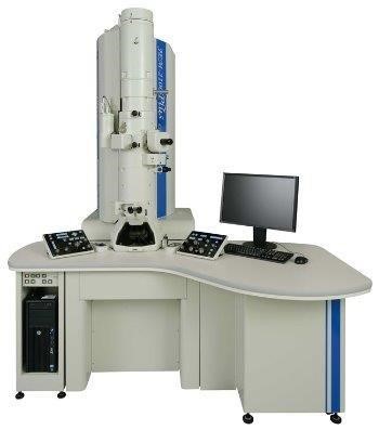
Transmission Electron Microscope (TEM)

is a microscopic technique that uses a beam of electrons that passes through an ultra-thin specimen.
The TEM offers much higher resolution than the optical microscope due to the small wavelength of electrons, allowing users to examine sample details with atomic-level precision — down to a single row of atoms. This microscope can magnify images up to ten thousand times more than a light microscope.
The transmission electron microscope represents an essential analytical tool in many branches of natural science, such as materials science, semiconductor research, as well as biological sciences, including virology and cancer research.
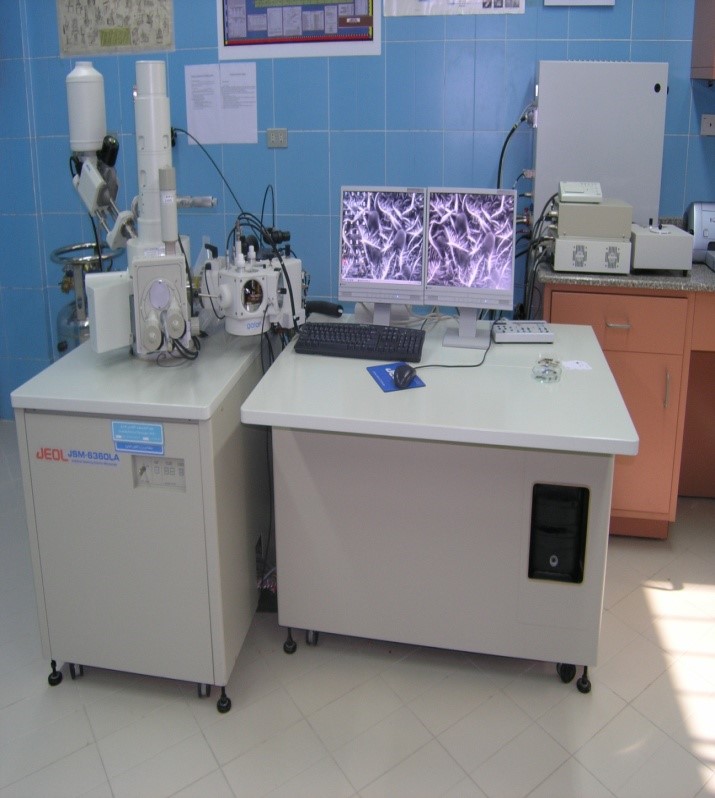
Scanning Electron Microscope (SEM)
Coating Device
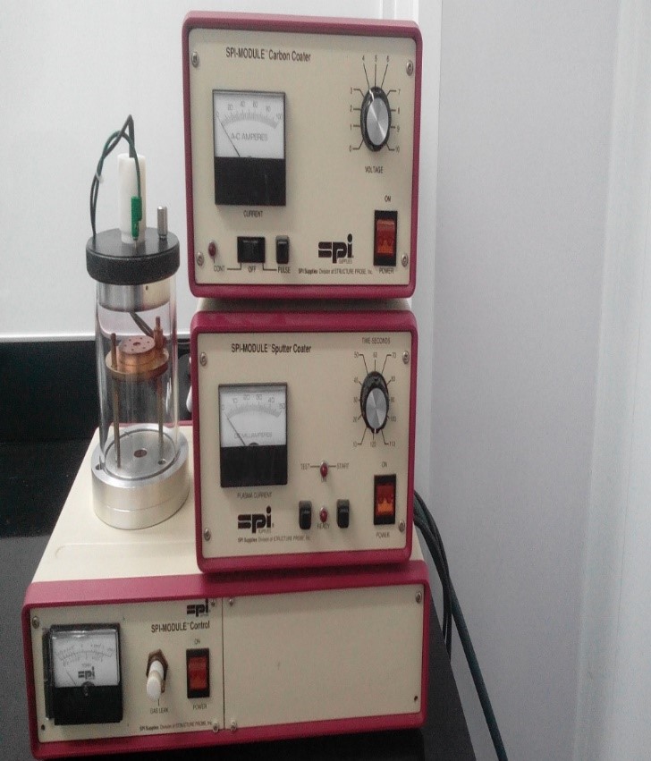
This device is used to increase the electrical conductivity of a sample by coating it with a thin layer of pure gold.
Advantages:
- Reduces beam damage during microscopy.
- Improves thermal conductivity.
- Enhances electrical conductivity.
- Improves secondary electron emission.
- Protects beam-sensitive samples.
- Reduces electron beam penetration.
Optical Microscope
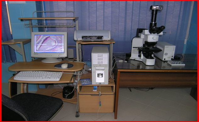
- Equipped with two light sources, allowing imaging of both transparent and opaque samples, making it suitable for biological and materials science applications.
- Features a digital camera and software that allows overlaying magnification labels on images and performing various measurements.
- The microscope operates automatically and includes a 100× air objective lens that does not require immersion oil.
Applications include:
Materials science, medicine, geology, marine sciences, environmental studies, and biological research.
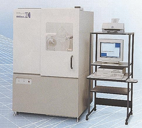
X-ray Diffraction (XRD) Device